

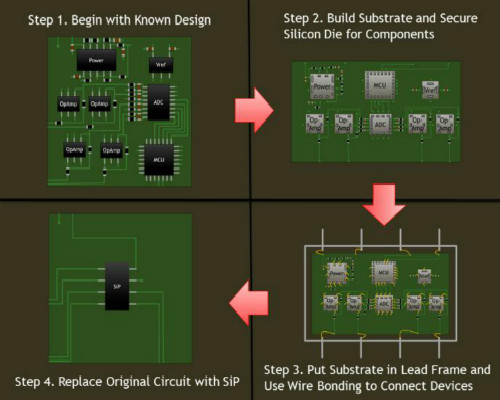
The most common packaging method for SIP is using ball grid array (BGA) technology, but there are complexities with using this or any other packaging method. From a circuit design perspective, the 3D chip packaging will have multiple die stacks, so this creates complications in how to layout the packaging.

When we doing these designs, Bi takes considerations about such arrangements, once solutions are taken, will be simulated with complex software to ensure system performance. This is key since the actual process of fabrication is complex and the design should be well understood before proceeding.
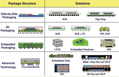
Bi SiP solutions leverage upon established IC assembly capabilities including copper wiring, flip chip packaging, wafer level packaging, fan-out wafer level packaging, 2.5D/3D IC and embedded chip packaging to address ongoing trends in mobile, IoT (Internet of Things), high performance computing, automotive, and artificial intelligence.